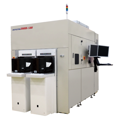
✔ INSPECTRA® 系列满足半导体前后段制程高速、高精度的全自动检测需求!
✔ Toray 独家 Die-to- Statistical-Image的比较技术可有效降低缺陷检测过程中造成的损坏及误判率。
|
产品功能
|
功能特点
|
应用效益
|
|---|---|---|
|
高分辨率的大范围检测
|
速度快,敏感度高
|
良好检测结果的高生产力
|
|
Die-to-Statistical-Image 算法
|
达成缺陷检测目标
|
控制流程变异及误宰
|
|
多款光学及硬件系统
|
提供光学检测解决方案
|
适用多种晶圆尺寸及晶圆种类
|
|
项目
|
规格
|
|---|---|
|
适用晶圆尺寸
|
2 ~ 12吋硅晶圆/带框晶圆/化合物晶圆/玻璃晶圆等
|
|
缺陷检出尺寸
|
> 0.5 μm
|
|
应用范围
|
正面/背面/边缘
|
|
应用领域
|
大规模集成电路(LSI)、影像传感器(CIS)、微机电(MEMS)、LED、凸块(Bump)、直通硅晶穿孔(TSV)检测、电源芯片、功率组件(SiC)、氮化镓(GaN)、化合物半导体
|

The corporate philosophy of the Toray Group is contributing to society through the creation of new values.
TASMIT, a member of Toray Engineering Group, executes this corporate philosophy with the aim of becoming a company that is highly valued by all of its stakeholders including customers, shareholders and employees.
To do this, TASMIT will contribute to solving social issues through its business and implement the idea of Creating Shared Value (CSV), which combines social values with corporate values.
TASMIT promises to provide effective solutions for the semiconductor device manufacturing with our two core technologies: optical wafer inspection "Inspectra" and electron wafer pattern inspection "NGR".