|
Model Number
|
SP3055S
|
||
|---|---|---|---|
|
Model Name
|
JadeSA-WBG, non-contact whole wafer / microarea 3D stress inspection and analysis system for SiC substrate, SiC on SiC, GaN on Si, GaN on SiC, GaN substrate
|
||
|
SiC Substrate /
EPI Wafer Size
|
2” 4” 6” 8”
|
||
|
Inspection Items
|
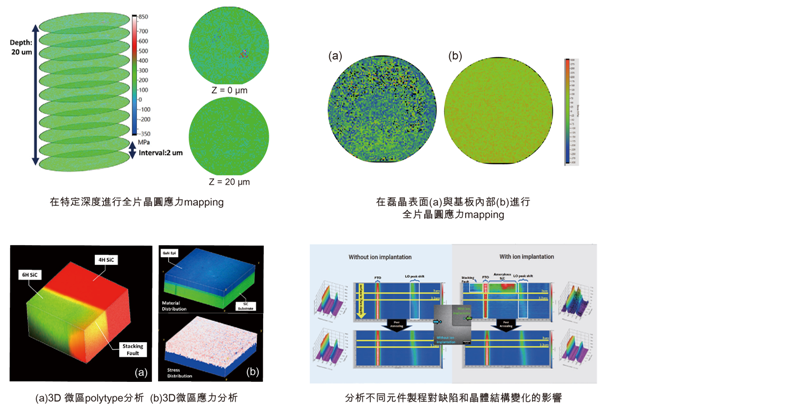
Whole wafer stress mapping MicroArea stress mapping
Polytype detection (4H, 6H, 3C SiC)
|
||
|
Whole Wafer
Stress Mapping
|
Estimated Inspection Time
|
2 mm Step Size
|
40 mins / layer (4”)
1.5 hrs / layer (6”)
|
|
1 mm Step Size
|
2 hrs / layer (4”)
4.5 hrs / layer (6”)
|
||
|
Axial Resolution
|
1 μm
|
||
|
Min. Step Size of XY Plane
|
0.1 mm
|
||
|
Max. Step Size of XY Plane
|
5 mm
|
||
|
XY Stage Repeatability
|
0.1 μm
|
||
|
Min Increment of Z Stage
|
0.02 μm
|
||
|
Analysis
|
Whole wafer stress analysis
Polytype Detection
|
||
|
MicroArea
Stress Mapping
|
Field of View
|
250 μm
|
|
|
Mapping Resolution
|
Up to 512 x 512
|
||
|
Lateral Resolution
|
0.3 μm
|
||
|
Axial Resolution
|
1 μm
|
||
|
Min Increment of Z Stage
|
0.02 μm
|
||
|
Analysis
|
MicroArea stress analysis
Polytype detection
|
||

南方科技成立於2014年8月,創辦團隊集合了光學、材料、物理、資訊等跨領域人才,將新穎的光學設計觀念導入光學工程領域。透過先進光學簡單化、模組化、數位化的核心理念,使研究人員專注在研究開發工作,改善實驗設計觀念、提升研究效率、縮短研發時程、揮灑研發創意,加速研究與產業技術發展的進程。南方科技以『5D顯微術』與『數位光學』兩大核心技術為基礎,將嶄新的光學觀念與技術導入先進材料分析、生醫影像、顯微3D光學檢測與數位光學應用四大應用領域。在不同的應用領域,南方致力於研發與創新,深入瞭解行業痛點並且專注解決關鍵問題。